In April I had the privilege of attending a three-day course on Electromagnetic Compatibility (EMC) Engineering taught by Henry Ott, the author of the book on the subject with the same title. EMC is the branch of electrical engineering concerned with the unintentional generation, propagation and reception of electromagnetic energy which may cause unwanted effects such as electromagnetic interference (EMI) or even physical damage in operational equipment [1]. Ott’s book is a treasure trove of practical advice on the subject, so I arrived with high hopes.
I was not disappointed. Electromagnetic compatibility is often described as ‘black magic’, so getting an intuition for the subject is a valuable asset. One of the first things out of Mr. Ott’s mouth was a statement about how the semantics of EMC often prevents understanding. We got right into breaking down the theory into clear intuition-building units.
The seminar focused on a wide variety of topics including:
- Proper cabling shielding and noise immunity
- Grounding principles
- Digital layout and grounding
- High-speed digital decoupling
- Radiated emission control
- Digital transmission lines
- Mixed signal PCB grounding and layout
- RF and transient immunity
- Conducted emission control
- Shielding principles and applications
In this blog post, I’ll go into detail on the first topic listed above.
Simplexity’s focus on mechatronics means we deal with systems that include both motors with relatively high current, and analog sensors which are susceptible to the noise created by the motors. Additionally, motors are controlled with pulse width modulation, which uses a square wave signal that includes high frequency components which can couple into susceptible circuits. A key part of a mechatronic design is knowing how to prevent noise coupling.
The first thing to realize is what is the source of the noise voltage you would like to prevent, and what is the receiver element in your circuit. Is it electrically (capacitive) coupling into your system, or magnetically (inductive) coupling? The model for each type can help understand the source and the cure.
- VN=jwRC12V1 (capacitive coupling)
- VN=jwBAcosƟ = jwM12I1 (inductive coupling)
In each case there is a source signal in the form of a voltage or current (V1 or I1). This source signal has a characteristic frequency, which gives us the jw term in the equations above. Because this signal is either required by another part of the system, or not under your control (in the case of noise coming from someone else’s circuitry) you can’t really do much to affect the size of the noise voltage (VN) with these terms.
So, we turn to the part of the equation that deals with where the noise voltage is being picked up. In both cases, we are dealing with a parasitic element. In the first case, by C12, the capacitance between the noise source and your cable multiplied by the resistance in the cable; and, in the second by M12, the mutual inductance between the inductance of the noise source and the inductance in the cable of interest. The second expression is also shown in another form because it is easier to understand the components of the relationship, and therefore how to minimize them. For that expression the magnetic field, B, and the area of path of the current, A, and the orientation between the field and the loop, Ɵ are used.
Inductive coupling is common when motors are involved because they usually require a relatively high current. Looking at the expression (2), we see the only way to reduce the noise voltage VN (without reducing the current or frequency needed to drive the motor) is to reduce the magnetic field, B, created by the noise source, or by reducing the pick-up of the B field in the cable of interest.
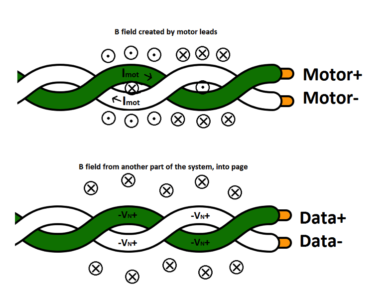
To reduce the magnitude of the magnetic field, B, we can use a twisted pair. The magnetic field is created by the changing current in the wire. If we twist the motor supply current wire around its return path, looking at the top figure in the diagram below we see the magnetic field from one loop is in the opposite direction to the one next to it, canceling it out and reducing the effect it has on nearby wires.
Similarly, on the other end of the system, we can reduce the pick-up of the magnetic field by reducing the area of the signal path of the cable, A. This means either running the cable close to a ground plane, or, if you know that the signal’s return path is through a neighboring wire, you can use the same twisted pair to keep the area minimized, and any noise voltage picked up on each loop will be cancelled by the noise voltage picked up by the other cable (see the lower figure in the diagram below). Note that the signals on the two wires in the twisted pair must be equal, but flowing in the opposite direction. Also, the pitch of the twist should be smaller than 1/20th of the wavelength of the frequency of the noise signal. It is pretty easy to find wire that is twisted at least as tightly as 1 turn/inch, which would be a valid choice for reducing noise at frequencies of up to 500MHz.

Figure 1. Twisted pair diagram in context of generating magnetic fields (top) and picking-up noise in the presence of an externally created magnetic field.[2]
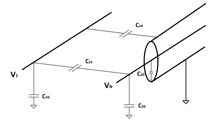
If you consider that the noise coupling is based on the capacitance between the noise source conductor and the conductor of interest, how does shielding reduce this number? The key is not in the shielding itself, but in the way that that shield is terminated. If we ground the shield, then the capacitance between the shield and the conductor of interest becomes a capacitance to ground. C12 now is only due to the fact that your conductor must stick out from inside the cable at the end. You have effectively reduced the area of overlap significantly, and therefore reduced the noise coupling of your signal.
In this way, Mr. Ott emphasized that the key to shielding properly is to terminate your cable properly. The shield must be grounded and care should be taken to electrically connect the shield to any connectors used and to the box enclosure. In his book, ‘Electromagnetic Compatibility’ he goes into more detail on all of these items, and on when a shielded cable can help with magnetic noise issues as well (hint: the key is still in reducing loop area).
Keeping the expressions for noise voltage in mind when considering how to improve the noise immunity of your system can really help get an intuitive sense of when different methods of cable shielding and the use of twisted pairs is useful. The Electromagnetic Compatibility Seminar taught by Henry Ott was full of these sorts of lessons, marrying the art of the ‘rule of thumb’ with the rigor of theory, resulting in the dispelling of the myth of the ‘black magic’ of electromagnetic radiation control.
[1] Definition of EMC from Wikipedia: https://en.wikipedia.org/wiki/Electromagnetic_compatibility
[2] Diagram of twisted pairs from Wikipedia: https://upload.wikimedia.org/wikipedia/commons/c/c2/USB_Twisted_Pair.svg


